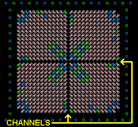
| Channel Routing is a patented process used to create additional routing escape paths within a BGA fanout pattern. By creating the additional routing channels, the BGA can be routed with a fewer layers, reducing the overall PCB cost. |
|

|
| Figure 1 -- Top Layer | Figure 2 -- Inner Layer with Channel Routing |
|
The Channels are created using regular sized vias, that are either laser or mechanically
drilled, one or two layers deep, during the normal PCB fabrication process. On subsequent
layers, additional routing escape channels have been created.
|