
|
|
|
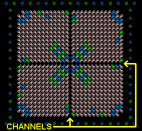
| Figure 1 -- Top Layer | Figure 2 -- Inner Layer with Channel Routing |
| Q. | 1) What's A Channel ? |
| A. |
Imagine a BGA footprint divided into four equal quadrants with pins fanned
out into four different directions. The pattern of vias under the BGA would
appear to have two wide routing "channels" forming a cross. (See figure 1)
This cross pattern, is the standard way to fanout most BGA’s. |
| Q. | 2) What's the problem ? |
| A. |
With high pin count BGA’s, it takes more and more layers to connect the
fanned out pins to the rest of the circuit board. In theory, a 1600 pin
(40x40) BGA has 156 possible routes per layer (1 trace between vias) plus 20
traces in the channels. This means that 9 layers would be required simply to
connect the BGA to the rest of the circuit. High layer and high via count
and high via aspect ratio makes PCB board fabrication more difficult and
expensive. |
| Q. | 3) What's the Solution ? |
| A. |
If we create more routing channels, we connect more traces per layer and can
reduce the total layer count. Channel Routing uses micro vias and pin
sharing to form additional cross shaped channels in the BGA fanout pattern.
(See figure 2). The new channels allow for 5 extra escapes per
channel. In addition, if we use via sharing on power pins and do not fanout
unconnected pins, the BGA becomes more open and easy to route. Up to four
(4) routing layers can be eliminated, lowering the cost of the PCB. |
| Q. | 4) Do I have to buy the software ? |
| A. |
No, the software is not required, it only speeds up the process of locating
and creating the channel inside the BGA fanout pattern. However, A signed
license agreement is still required, even if you plan to create the channels manually.
|
| Q. | 5) Do I have to use Micro Vias ? |
| A. |
Channels can be created using regular sized vias, that are either laser or mechanically
drilled, one or two layers deep, during the normal PCB fabrication process. This adds up
to three percent to the board cost (for the same number of layers), but channel routing
eliminates 2, 4, 6 or more layers, increasing manufacturing yield and reducing overall board costs. |
| Q. | 6) Which versions of Cadence do you support ? |
| A. |
Currently we support Cadence Allegro versions 13.6, 14.2, 15.0 and 15.1. We are also beta
testing version 15.2. |
| Q. | 7) What if I use Mentor, Zuken or Pads ? |
| A. | At this time, the automated Channel Routing software tool is only available
for the Cadence Allegro CAD tool. Channel Routing can be done
manually without the automated software, however, it can take up to a
week or more to fan-out one BGA. Also see Q8 below. (Call us for documentation and training) |
| Q. | 8) Can the Channel Routing program run on my platform ? |
| A. |
The Channel Routing Skill program is compatible with HP and Sun machines running HPUX 10.20, 11.0
and Solaris 8 (2.8). On the PC machines, the Channel Routing program is compatible with NT4.0,
Windows 2000 and Windows XP. |
| Q. | 9) Do I Need A License ? |
| A. |
The Channel Routing process is patented (US Patent # 6,388,890 Among others, plus patents pending in other countries). Use of Channel Routing requires a software license (for automated software tool users) and the PCBs are manufactured under license. (Call us for information) |
| Q. | 10) How can I see a demonstration ? |
| A. |
We can set up a live, interactive demonstration, directly to your PC or UNIX workstation.
For an appointment Call Us to arrange a time. OR You can download a quick video demonstration in RealPlayer 9 format, Here. (16 meg, 10 minutes in length) |
| Q. | 11) Can I download a brochure ? |
| A. |
Yes, Just click Here to download the Channel Routing brochure.
|
| Q. | 12) Can I see some Channel Routing examples ? |
| A. |
Yes, Just click Here to download a PDF file showing some Channel Routing examples.
|